
Focused Ion Beam Market Outlook: Semiconductor Innovation and Precision Analysis Growth Opportunities
The focused ion beam market is witnessing strong growth, driven by increasing demand for advanced semiconductor manufacturing, nanotechnology research, and high-precision material analysis.

According to IMARC Group's latest research publication, The global focused ion beam market size reached USD 1,102.4 Million in 2024. Looking forward, IMARC Group expects the market to reach USD 1,766.0 Million by 2033, exhibiting a growth rate (CAGR) of 5.38% during 2025-2033.
How AI is Reshaping the Future of Focused Ion Beam Market
- Automated Feature Recognition and Milling Navigation: AI systems integrate machine learning for automated defect identification and milling pathway optimization, reducing operator dependency by 40-50% for standardized workflows while improving processing speed and accuracy.
- Real-Time Beam Parameter Optimization: AI-driven algorithms dynamically adjust ion beam parameters including current, spot size, and scan patterns based on monitored environmental factors, maximizing precision while minimizing material damage during nanofabrication processes.
- Predictive Equipment Maintenance and Quality Control: Machine learning analyzes sensor data from FIB systems to predict component failures before breakdowns occur, reducing downtime and ensuring continuous production while detecting quality deviations with computer vision technology.

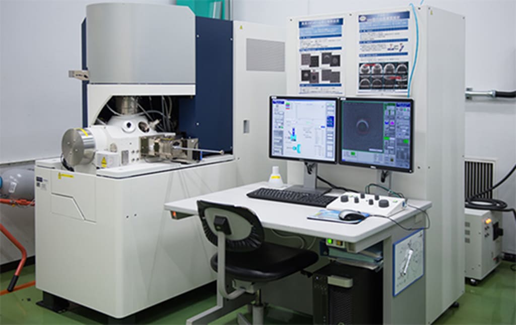
Focused Ion Beam Industry Overview:
The semiconductor industry's push toward sub-3nm nodes is revolutionizing FIB demand globally. TSMC began mass production of 2nm chips in second half 2025 using gate-all-around nanosheet transistors, while Samsung launched its 2nm Exynos 2600 processor in December 2025. These advanced nodes require exceptionally precise failure analysis, circuit editing, and cross-sectional imaging capabilities that only FIB systems can provide, driving robust equipment procurement from foundries worldwide.
Focused Ion Beam Market Trends & Drivers
Advanced semiconductor manufacturing complexity is the primary force propelling FIB market expansion. The transition from 3nm to 2nm process nodes requires gate-all-around transistor architectures with over 1,000 processing steps across 70-90 days of fabrication time. TSMC's 2nm wafers cost approximately tens of thousands of dollars each, making failure analysis and defect detection mission-critical. In March 2025, ZEISS introduced the Crossbeam 550 Samplefab next-generation FIB-SEM system that prepares up to 10 lamellae in less than eight hours, establishing new efficiency standards for semiconductor analysis and accelerating adoption across major foundries.
Integration of automation and artificial intelligence technologies is transforming FIB operational efficiency across all end-use industries. Service providers implementing AI-assisted milling protocols report 40-50% reductions in processing time for standardized workflows while maintaining quality standards. Hitachi High-Technologies unveiled FIB systems integrating artificial intelligence to optimize ion beam parameters in real-time, addressing key pain points around reproducibility and operator skill requirements. These intelligent systems enable smaller laboratories and research facilities to access advanced nanofabrication capabilities previously requiring highly specialized personnel, democratizing FIB technology access and expanding the addressable market.
Battery technology development and emerging nanotechnology applications are creating substantial new growth avenues beyond traditional semiconductor markets. FIB-SEM systems have become essential for analyzing battery component microstructures, investigating failures, and optimizing performance in electric vehicle and energy storage applications. TESCAN ORSAY HOLDING supplied AMBER X FIB-SEM systems to Germany's Institute for Factory Automation and Production Systems for battery research. Meanwhile, life sciences applications are expanding rapidly, with Thermo Fisher Scientific launching Hydra Bio with plasma-focal ion beam in September 2023 to streamline volume electron microscopy for cell biologists, and EMBL partnering with ZEISS in July 2023 to advance imaging technologies for biological research.
Leading Companies Operating in the Global Focused Ion Beam Industry:
- A&D Company, Limited
- Eurofins Scientific
- Hitachi High-Tech Corporation
- JEOL Ltd.
- RAITH GmbH
- Tescan Group a.s.
- Thermo Fisher Scientific Inc.
- Veeco Instruments Inc.
- ZEISS Microscopy
- zeroK NanoTech
Focused Ion Beam Market Report Segmentation:
By Ion Source:
- Ga+ Liquid Metal
- Gas Field
- Plasma
Ga+ liquid metal represents the largest segment, accounting for over 80% market share due to its high precision, widespread adoption in semiconductor failure analysis, and established reliability in industrial applications.
By Application:
- Failure Analysis
- Nanofabrication
- Device Modification
- Circuit Edit
- Others
Failure analysis exhibits clear dominance in the market as semiconductor manufacturers increasingly rely on FIB systems for defect identification, quality assurance, and troubleshooting in advanced chip production.
By End Use:
- Electronics and Semiconductor
- Industrial Science
- Bioscience
- Material Science
- Others
Electronics and semiconductor holds the largest market share owing to the growing complexity of chip manufacturing, transition to sub-5nm nodes, and critical need for precise circuit modification and photomask repair.
Regional Insights:
- North America (United States, Canada)
- Asia Pacific (China, Japan, India, South Korea, Australia, Indonesia, Others)
- Europe (Germany, France, United Kingdom, Italy, Spain, Russia, Others)
- Latin America (Brazil, Mexico, Others)
- Middle East and Africa
North America dominates the focused ion beam market with 34.7% revenue share due to its rapidly growing semiconductor industry, robust research infrastructure, and substantial governmental support through the CHIPS and Science Act.
Recent News and Developments in Focused Ion Beam Market
- March 2025: ZEISS introduced the Crossbeam 550 Samplefab, a next-generation FIB-SEM system transforming TEM sample preparation in electronics and semiconductors. The automated system prepares up to 10 lamellae in less than eight hours without manual intervention, achieving thinning down to 100 nm on various semiconductors and establishing new standards for efficiency and reliability.
- December 2025: Samsung Electronics officially launched the world's first mobile application processor Exynos 2600 fabricated using 2nm process technology. The chip adopts a ten-core design based on Arm's latest architecture, with CPU computing performance improved up to 39% compared to previous generation, demonstrating advanced process capabilities.
- Second Half 2025: TSMC entered mass production of 2nm process technology as scheduled, with plans for widespread use in supercomputers, mobile devices, and cloud data centers. The 2nm process offers 10-15% speed improvement at same power level or 25-30% power reduction at same speed compared to 3nm.
- September 2024: Thermo Fisher Scientific launched Thermo Scientific Hydra Bio with plasma-focal ion beam (PFIB), streamlining volume electron microscopy procedures for cell biologists working with resin or cryo-enclosed samples. The system integrates into Helios Hydra DualBeam Platform supporting various microscopy technologies.
- July 2023: European Molecule Biology Institute (EMBL) and ZEISS announced partnership to develop life sciences imaging technologies. The collaboration provides EMBL Imaging Centre users access to latest ZEISS microscope technology while EMBL research provides insights for ZEISS product enhancement.
Note: If you require specific details, data, or insights that are not currently included in the scope of this report, we are happy to accommodate your request. As part of our customization service, we will gather and provide the additional information you need, tailored to your specific requirements. Please let us know your exact needs, and we will ensure the report is updated accordingly to meet your expectations.
About the Creator
James Whitman
With years of experience in analyzing global industries, I specialize in delivering actionable market insights that help businesses stay ahead in an ever-changing landscape.
Keep reading
More stories from James Whitman and writers in Futurism and other communities.
Pouches Market Outlook: Flexible Packaging Demand and Sustainable Growth Opportunities
According to IMARC Group's latest research publication, The global pouches market size reached USD 54.7 Billion in 2024. Looking forward, IMARC Group expects the market to reach USD 83.2 Billion by 2033, exhibiting a growth rate (CAGR) of 4.53% during 2025-2033.
By James Whitman2 days ago in Futurism
Specialty Food Ingredients Market Outlook: Clean Label Innovation & Future Demand
According to IMARC Group's latest research publication, the global specialty food ingredients market size reached USD 85 Billion in 2024. Looking forward, IMARC Group expects the market to reach USD 126 Billion by 2033, exhibiting a growth rate (CAGR) of 4.5% during 2025-2033.
By sujeet. imarcgroup8 days ago in Futurism
Agricultural Adjuvant Market Outlook: Spray Efficiency Technologies & Future Demand
According to IMARC Group's latest research publication, global agricultural adjuvant market size reached USD 4.0 Billion in 2024. Looking forward, IMARC Group expects the market to reach USD 6.6 Billion by 2033, exhibiting a growth rate (CAGR) of 5.14% during 2025-2033.
By sujeet. imarcgroup5 days ago in Futurism


Comments
There are no comments for this story
Be the first to respond and start the conversation.